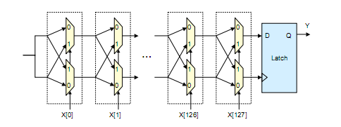
电路图的描述如下
Figure 1 illustrates a silicon PUF delay circuit based on
MUXes and an arbiter. The circuit has a multiple-bit input
X and computes a 1-bit output Y based on the relative delay
di?erence between two paths with the same layout length.
The input bits determine the delay paths by controlling the
MUXes. Here, a pair of MUXes controlled by the same input
bit X[i] work as a switching box (dotted boxes in the ?gure).
The MUXes pass through the two delay signals from the left
side if the input control bit X[i] is zero. Otherwise, the top
and bottom signals are switched. In this way, the circuit can
create a pair of delay paths for each input X.Toevaluate
the output for a particular input, a rising signal is given to
both paths at the same time, the signals race through the
two delay paths, and the arbiter (latch) at the end decides
which signal is faster. The output is one if the signal to the
latch data input (D) is faster, and zero otherwise.
大部分能理解,可是中间这个MUX如何工作的无法理解,MUX不是数据选择器吗,在这里如何使用啊。
------解决思路----------------------
用于数字延时路径的举例而已